Rigid-Flex Boards PCB Layout Design Designability Automotive Electronics
PCB Layout Design Description:
1. PCB design type: High-Speed, Analog, Digital-analog Hybrid, High Density/Voltage/Power, RF, Backplane, ATE, Soft Board, Rigid-Flex Board, Aluminum Board, etc.
2. Design tools: Allegro, Pads, Mentor Expedition.
PCB Layout Design Parameters:
| SMT Capability | 14 million spots per day |
| SMT Lines | 12 SMT lines |
| Reject Rate | R&C: 0.3% |
| IC: 0% |
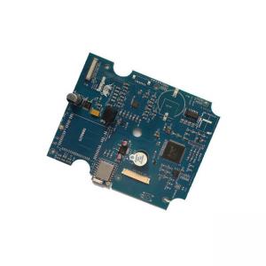
| PCB Board | POP boards/Normal Boards/FPC boards/Rigid-flex boards/Metal base boards |
| Parts Dimension | Min BGA Footprint:03015 Chip/0.35mm BGA |
| Parts SMT Accuracy:±0.04mm |
| IC SMT Accuracy:±0.03mm |
| PCB Dimension | Size:50*50mm-686*508mm |
| Thickness: 0.3-6.5mm |
PCB Layout Design Introduction:
1. Under normal circumstances, all components should be arranged on the same side of the circuit board. Only when the top components are too dense, can some devices with limited height and low heat generation, such as chip resistors, chip capacitors, Chip IC, etc. are placed on the bottom layer.
2. On the premise of ensuring electrical performance, components should be placed on the grid and arranged in parallel or perpendicular to each other to be neat and beautiful. In general, components are not allowed to overlap; the arrangement of components should be compact, and components should be placed on the entire layout. The distribution is uniform and the density is consistent.
3. The minimum spacing between adjacent pad patterns of different components on the circuit board should be more than 1MM.
4. The distance from the edge of the circuit board is generally not less than 2MM. The best shape of the circuit board is a rectangle, and the aspect ratio is 3:2 or 4:3. When the surface size of the circuit board is greater than 200MM by 150MM, it should be considered that the circuit board can withstand Mechanical strength.